HDI (High Density Interconnect)
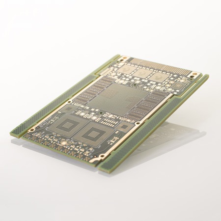
Advances in technology have enabled products to deliver enhanced performance in smaller form packaging. The adoption has become widespread, touching the majority of global markets. The miniaturization of components and semiconductor packages that supports advanced features invariably drives the technology of the PCB, giving rise to the use of fine features, high performance thin materials and laser-drilled blind or buried microvia technology. Microvias allow the use of micro-interconnects from one layer to another within a PCB utilizing a smaller pad diameter creating additional routing density.
FEATURES AND BENEFITS
* 1+N+1 – PCBs contain 1 of high-density interconnection layer.
* 5+N+5: PCBs contain 5 levels of high density interconnection layers. Microvias on different layers can be staggered or stacked. Copper filled stacked microvia structures are commonly seen in demanding designs. [Any Layer HDI: All the layers of a PCB are high density interconnection layers which allows the conductors on any layer of the PCB to be interconnected freely with copper filled stacked microvia structures.